Electron Microscopes
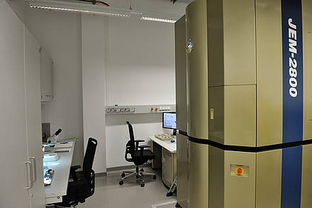
S/TEM Jeol JEM2800
- Electron gun: Schottky Field Emission
- Accelerating voltage: 100 kV, 200kV
- Imaging modes:
- Transmission electron microscopy
- Scanning transmission microscopy
- bright-field detector
- dark-field detector
- secondary electrons detector
- Energy-dispersive X-ray spectroscopy detector Jeol Centurio: large solid angle silicon drift detector with 100mm2 active area for ultrafast elemental mapping of S/TEM samples
- 3D tomography (TEMography software – recorder, composer, visualizer)
- TEM camera OSIS Veleta
- CMOS TEM camera TemCam-XF416 (EM-Menu SW, EM-Tools SW)
- Universal Scan Generator TVIPS with EMScan SW
- SerialEM SW
- Single-tilt holder
- Double-tilt EDS dedicated holder
- Multigrid-single-tilt holder (3 grids)
- Double-tilt in situ MEMS-based heating holder Protochip Fusion Select
- 3D tomography (TEMography software – Recorder, Composer, Visualizer)
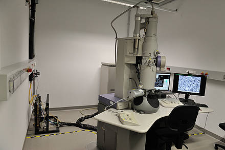
TEM Tecnai 10
- Electron gun: LaB6
- Accelerating voltage: 80kV, 100kV
- Imaging mode: Transmission electron microscopy
- TEM camera OSIS Megaview G3
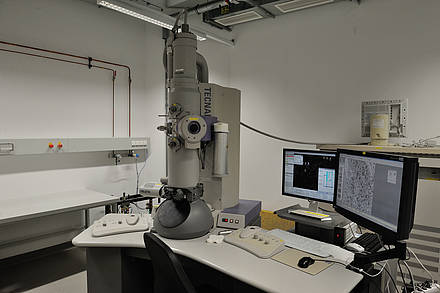
TEM Tecnai 12
- Electron gun: LaB6
- Accelerating voltage: 100 kV, 120 kV
- Imaging mode: Transmission electron microscopy
- TEM camera OSIS Veleta
- Cryo Transfer System for observation of frozen samples
- SerialEM SW
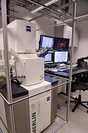
FE-SEM Merlin VP Compact + ATLAS Array Tomography
Accelerating voltage: 0.02 to 30kV
Resolution:
- 0.8 nm @ 15 kV
- 1.6 nm @ 1 kV
- 0.8 nm @ 30 kV (STEM mode)
Probe current: up to 20nA
Vacuum modes:
- High Vacuum
- Variable pressure up to 60 Pa
Detectors:
- High efficiency secondary electron detector HE-SE2 – Everhart-Thornley type
- In-lens Duo detector – combination of In-lens SE and In-lens BSE imaging
- Scanning transmission electron microscopy detector
- Variable pressure secondary electron detector
- Cathodoluminescence detector for material characterization
- EDS detector: Octane Elite EDS System with 70 mm2 chip and silicon nitride (Si3N4) window
5-axes mot. eucentric stage with dual joystick controller
Plasma Cleaner for gentle removal of sample contamination
Local Charge Compensation for undisturbed imaging of non-conductive samples and in situ cleaning of sample surface
ATLAS Array Tomography for 3D reconstruction of sample data